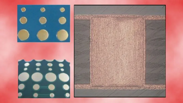
Ideal for applications where cooling fans or heatsinks aren’t practical.
Neat idea! I bet it’s expensive though.
Is there a particular reason this can’t be done as layers are deposited?
Takes a long time and risks creating voids that offgas or pop during reflow. Currently there are options for conductive copper filled epoxies. This appears to use a combination of copper slugs / disks and chemical deposition to save time and avoid voids in the larger central area.
One thing to know is that the spaces below components like CPUs are frequently filled with holes that connect the part to other parts on the PCB. They’re called vias. This is because they have too high a pin density to connect all of them on a single layer.
Still, perhaps the sizes of the via pads could be adapted to these findings? Using vias to dissipate heat on other parts is fairly common, but I don’t know if current standards are as efficient as this.


